Полезное:
Как сделать разговор полезным и приятным
Как сделать объемную звезду своими руками
Как сделать то, что делать не хочется?
Как сделать погремушку
Как сделать так чтобы женщины сами знакомились с вами
Как сделать идею коммерческой
Как сделать хорошую растяжку ног?
Как сделать наш разум здоровым?
Как сделать, чтобы люди обманывали меньше
Вопрос 4. Как сделать так, чтобы вас уважали и ценили?
Как сделать лучше себе и другим людям
Как сделать свидание интересным?

Категории:
АрхитектураАстрономияБиологияГеографияГеологияИнформатикаИскусствоИсторияКулинарияКультураМаркетингМатематикаМедицинаМенеджментОхрана трудаПравоПроизводствоПсихологияРелигияСоциологияСпортТехникаФизикаФилософияХимияЭкологияЭкономикаЭлектроника
Tight-binding model and edge states
|
|
There are two typical shapes of a graphene edge, called armchair and zigzag. The two edges have 30◦ difference in their cutting direction. Here we briefly discuss the way that the graphene edges drastically change the π-electronic structures [7]. In particular, a zigzag edge provides the localized edge state, while an armchair edge does not show such localized states.
A simple and useful model to study the edge and size effect is one of the graphene ribbon models as shown in figures 1(a) and (b). We define the width of graphene ribbons as N, where N stands for the number of the dimer (two carbon sites) lines for the armchair ribbon and by the number of the zigzag lines for the zigzag ribbon, respectively. It is assumed that all dangling bonds at graphene edges are terminated by hydrogen atoms, and thus make no contribution to the electronic states near the Fermi level. We employ a single-orbital tight-binding model for the π-electron network. The Hamiltonian is written as,
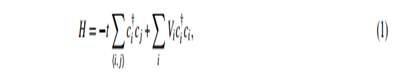
where the operator ci † creates a π-electron on the site i. h i, j i denotes the summation over the nearest-neighbor sites. t, the transfer integrals between all the nearest-neighbor sites, are set to be unity for simplicity. This is sufficient to show the intrinsic difference in the electronic states originating from the topological nature of each system. The value of t is considered to be about 2.75eV in a graphene system. The second term in equation (1) represents the impurity potential; V i = V (r i) is the impurity potential at a position r i. The effect of impurity potential on the electronic transport properties will be discussed in the next section.
Prior to the discussion of the π-electronic states of graphene nanoribbons, we shall briefly review the π-band structure of a graphene sheet [68]. To diagonalize the Hamiltonian for a graphene sheet, we use a basis of the two-component spinor, c k † = (c A† k, c B† k), which is the Fourier transform of (ci †∈A, ci †∈B). Let τ 1, τ 2 and τ 3 be the displacement vectors from a B site to its three
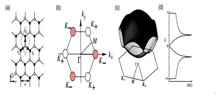
Figure 2. (a) A graphene sheet in real space, where the black (white) circles mean the A(B)-sublattice site.√  a =is the lattice constant. Here− √ τ 1 = (0, a /√3), τ 2 = (− a /2,− a /2 3), and τ 3 (a /2, a /2 3). (b) First BZ of graphene.
K  , K
, K  . (c) The π band structure and (d) the density of states of the graphene sheet. The valence and conduction bands make contact at the degeneracy point K ±.
nearest-neighbor A sites, defined so that z ˆ · τ 1 ×τ 2 is positive (figure 2(a)). z ˆ is the normal vector 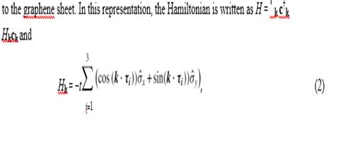
where σˆ = (σˆ x,σˆ y,σˆ z) are the Pauli matrices. Then, the energy eigenvalues are E k ± =
± t  . Since one carbon site has one π-electron on average, only the E k −-band is completely occupied.
In figures 2(b)–(d), the first Brillouin zone (BZ) of the graphene lattice, the energy dispersion of π-bands in the first BZ and the corresponding density of states are depicted, respectively. Near the 0 point, both valence and conduction bands have the quadratic form of kx and ky, i.e. E k = ±(3−3| k |2/4). At the M points, the middle points of the sides of the hexagonal BZ, the saddle point of energy dispersion appears and the density of states diverges logarithmically. Near the K point of the corner of the hexagonal first BZ, the energy dispersion
is linear in the magnitude of the wave vector, E k = ±√3 ta | k |/2, where the density of states
linearly depends on the energy. Here a (= √3|τ i |(i = 1,2,3)) is the lattice constant. The Fermi energy is located at the K points and there is no energy gap at these points, since E k vanishes at these points by hexagonal symmetry.
The energy band structures of armchair ribbons are shown in figures 3(a)–(c), for three different ribbon widths, together with the density of states. The wavenumber k is normalized by the length of the primitive translation vector of each graphene nanoribbon, and the energy E is scaled by the transfer integral t. The top of the valence band and the bottom of the conduction band are located at k = 0. It should be noted that the ribbon width decides whether the system is metallic or semiconducting. As shown in figure 3(b), the system is metallic when N = 3 M −1, where M is an integer. For semiconducting ribbons, the direct gap decreases with increasing ribbon width and tends to zero in the limit of very large N. For narrow nondoped metallic armchair nanoribbons, an energy gap can develop due to Peierls instabilities
Figure 3. Energy band structure E (k) and density of states D (E) of armchair ribbons of various widths ((a) N = 4, (b) 5 and (c) 30).
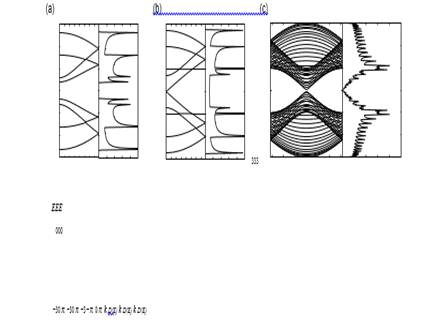
Figure 3. Energy band structure E (k) and density of states D (E) of armchair ribbons of various widths ((a) N = 4, (b) 5 and (c) 30).
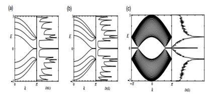
Figure 4. Energy band structure E (k) and density of states D (E) of zigzag ribbons of various widths ((a) N = 4, (b) 5 and (c) 30).
toward low temperatures [69], which is consistent with the recent density functional theory calculation [56, 70].
For zigzag ribbons, however, a remarkable feature arises in the band structure, as shown in figures 4(a)–(c). We see that the highest valence band and lowest conduction band are always degenerate at k = π. It is found that the degeneracy of the center bands at k = π does not originate from the intrinsic band structure of the graphene sheet. These two special center bands get flatter with increasing ribbon width. A pair of partial flat bands appears within the region of 2π/3 6 | k | 6 π, where the bands sit in the vicinity of the Fermi level.
The electronic state in the partial flat bands of the zigzag ribbons can be understood as the localized state near the zigzag edge by examining the charge density distribution [7]–[9], [11, 12]. Here we show that the puzzle for the emergence of the edge state can be solved by considering a semi-infinite graphite sheet with a zigzag edge. First, to show the analytic form, we depict the distribution of charge density in the flat band states for some wavenumbers in figure 5(a)–(d), where the amplitude is proportional to the radius. The wave function has nonbonding character, i.e. finite amplitudes only on one of the two sublattices, which includes the edge sites. It is completely localized at the edge site when k = π, and starts to gradually penetrate into the inner sites as k deviates from π reaching the extended state at k = 2π/3.
Considering the translational symmetry, we can start constructing the analytic solution for the edge state by letting the Bloch components of the linear combination of atomic orbitals
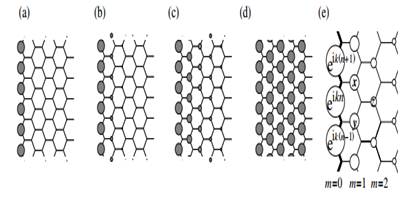
Figure 5. Charge density plot for analytic solution of the edge states in semiinfinite graphite, when (a) k = π, (b) 8π/9, (c) 7π/9 and (d) 2π/3. (e) An analytic form of the edge state for a semi-infinite graphite sheet with a zigzag edge, emphasized by bold lines. Each carbon site is specified by a location index n on the zigzag chain and by a chain order index m from the edge. The magnitude of the charge density at each site, such as x, y and z, is obtained analytically (see text). The radius of each circle is proportional to the charge density on each site, and a drawing is given for k = 7π/9.
(LCAO) wave function be..., ei k (n −1), ei kn , ei k (n +1),... on successive edge sites, where n denotes a site location on the edge. Then the mathematical condition necessary for the wave function to be exact for E = 0 is that the total sum of the components of the complex wave function over the nearest-neighbor sites should vanish. In figure 5(e), the above condition is ei k (n +1) +ei kn + x = 0, ei kn +ei k (n −1) + y = 0 and x + y + z = 0. Therefore, the wave function components x, y and z are found to be Dk ei k (n +1/2), Dk ei k (n −1/2) and Dk 2ei kn , respectively. Here Dk = −2cos(k /2). We can thus see that the charge density is proportional to Dk 2(m −1) at each non-nodal site of the m th zigzag chain from the edge. Then the convergence condition of | Dk | 6 1 is required, for otherwise the wave function would diverge in a semi-infinite graphite sheet. This convergence condition defines the region 2π/3 6 | k | 6 π where the flat band appears.
Date: 2015-05-09; view: 914; Нарушение авторских прав