Полезное:
Как сделать разговор полезным и приятным
Как сделать объемную звезду своими руками
Как сделать то, что делать не хочется?
Как сделать погремушку
Как сделать так чтобы женщины сами знакомились с вами
Как сделать идею коммерческой
Как сделать хорошую растяжку ног?
Как сделать наш разум здоровым?
Как сделать, чтобы люди обманывали меньше
Вопрос 4. Как сделать так, чтобы вас уважали и ценили?
Как сделать лучше себе и другим людям
Как сделать свидание интересным?

Категории:
АрхитектураАстрономияБиологияГеографияГеологияИнформатикаИскусствоИсторияКулинарияКультураМаркетингМатематикаМедицинаМенеджментОхрана трудаПравоПроизводствоПсихологияРелигияСоциологияСпортТехникаФизикаФилософияХимияЭкологияЭкономикаЭлектроника
Summary of lectures
Topic 1: Introduction. Nanocrystalline materials (4:00)
Plan of the lecture
1. Introduction.
2. The concept of nanomaterials.
3. The relevance of Manufacture of nano-and ultrafine materials.
In recent years, the rapid growth of scientific, industrial and commercial interest in a new class of materials, the purpose of which reflected the desire for miniaturization in the practice of construction of various objects. These materials have unusually strong crystal lattice and exhibit unique properties in the CIS called ultrafine materials (UDM), or ultra-systems (UDS), and in Western literature - nanostructured materials (NSM).
Currently, both of these terms are equivalent to this new class of materials referred to the size of the morphological elements of less than 100 nm. On geometrical features of these elements can be divided into volmernye atomic clusters and particles, one-and two-dimensional multilayers, coatings and daminarnye structure, three-dimensional bulk nanocrystalline and nanophase materials.
It is generally accepted that under the UDM or nanomaterials means or deliberately engineered or natural materials, in which one or more sizes are in the range of nanometers. This category also includes the so-called "nano-nano" composites that contain more than one phase, but the phase is less than 100 nm. A large variety of types of UDM with their common feature size allows you to combine them in one term "nanomaterial". It is now widely used ultrafine powders (UDP), which occupy more than 90% of the U.S. market UDM, nanofibers and nanowires, nanofilms and nanocoatings, and start getting more and more application of bulk nanomaterials and nanozernistye nanocrystalline (grain size less than 100 nm) [1 ].
Understanding of nanocrystals has been introduced in the scientific literature in the 80-ies Glyayterom H. (Germany) and, independently, actively developed in Russia ID Morohovym with employees.
In the former Soviet Union a major role in the study of the properties of nanomaterials, the development of new, technology acquisition and use (nanotechnology) played high school.
The relevance of Manufacture of nano-or ultrafine (AP) materials are defined by features of their physical and chemical properties that allow you to create materials with a qualitatively and quantitatively new properties for use in practice. This is due to the fact that the material is of such small size is of great importance quantum mechanics, and it fundamentally alters the mechanical, optical and electrical properties of the substance.
The first studies of nanomaterials have shown that they are changed, compared to conventional materials such fundamental characteristics as the specific heat capacity, elastic modulus, and the diffusion coefficient, magnetic properties, etc. Consequently, we can talk about the state of nanostructured solid, fundamentally different from conventional crystalline or amorphous.
An analysis of theoretical and experimental studies carried out to the end of the 70's, led to the conclusion of a special solid state UD different from traditional and amorphous materials, and a definition of this concept on the basis of physical nature. In this case, the nano-or UD materials include media or materials that are characterized as small size of the morphological elements that it is commensurate with one or more fundamental quantities of the substance (measuring the crystal lattice, etc.)
As the size of the grains or particles become smaller and smaller, an increasing fraction of the atoms is on the boundaries or free surfaces. Thus, when the size of the structural units of 6 nm and thickness of the surface layer one atom almost half of the atoms will be located on the surface. Since the fraction of surface atoms in the UD material is tens of percent, clearly manifested all the features of the surface states, and the division of properties in "bulk" and "surface" becomes, to some extent, arbitrary. The developed surface affects both the lattice and the electronic subsystem.
There are anomalies in the behavior of electrons, quasi-particles (photons, magnons) and other elementary excitations, which result in changes in the physical properties of the DM systems compared to bulk materials.
The behavior of UD materials are often determined by the processes at the grain boundaries. For example, can deform nanoceramics almost long enough to slip through the borders. But "superplasticity" strain is in a strong contrast to the fragile behaviors associated with conventional ceramics. Because of the large number of borders and, as a consequence, this - a lot of short diffusion distances nanometally and ceramics are used as solid-phase binding agent to connect with others (sometimes disparate) coarse-grained materials. It is known [1] that some ceramics have extremely low thermal conductivity. This allows their use as thermal barrier coatings.
Reducing the size of grains of metal from 10 microns to 10 nanometers gives strength increase of about 30 times. Adding to the usual nano powders for pressing the latter leads to a decrease in the pressing temperature, high strength products. With the use of diffusion bonding between the welded parts of a thin layer of suitable composition nanopowders allows welding of dissimilar materials, including some difficult-to-metal alloys with ceramics, as well as to reduce the temperature of diffusion bonding.
Scientific research on the subject has been held for more than 100 years ago. In 1861, chemist T. Graham used the term "colloid" to describe solutions containing particles with a diameter of 1 to 100 nm in the suspension.
The use of colloids can be considered one of the first applications of nanomaterials. Similarly, for a long time used such substances containing ultrafine particles such as aerosols, paint pigments, colorants steklokolloidnye metal particles.
In recent years came into use the concept of nanotechnology. This term refers to the process of obtaining nano-and ultrafine materials and technological processes of instruments, devices, structures using nanomaterials.
Scientific and technical direction to obtain and study the properties of UD materials formed in the former USSR in the 50 years of the twentieth century. In the nuclear industry received UD powders with a particle size of about 100 nm, which have been successfully used in the manufacture of highly porous membranes for the diffusion method of uranium isotope separation. In the 60 years for the Institute of the USSR was developed levitation method for UD powders. In the 70 years through the use of electrical explosion of conductors and plasma fusion range UD powders has been significantly expanded, developed chemical methods for the synthesis of nanopowders of iron and other metals and composites based on them.
In the 1980s, Germany had obtained consolidated nanocrystalline materials.
In the last decade in developed countries formed the scientific and technical direction "Nanoparticles, materials, technologies and equipment," which is the fastest growing in terms of finance in the world.
In 1980, the study of clusters containing less than 100 atoms. In 1985, Smiley and Kroto with a group of Spectrographic found evidence that the C60 carbon clusters (fullerenes) exhibit extraordinary stability. In 1991, S. Iijima reported the study of carbon-graphite tube filaments nanotubes.
Recommended Reading
1. New materials / VN Antsiferov, FF Bezdudny, LN Belyanchikov and others, ed. YS Karabasova, Ministry of Education of the Russian Federation. - Moscow: MISA, 2002. - 736 p.
2. New substances, materials and products made of them as objects of inventions: Directory / VI Blinnikov etc. - Moscow, Metallurgy, 1991. - 262 p.
3. Rzhevskaya SV Materials science. - M. Bauman, 2000. - 280.
4. Kulikov V.Yu. Textbook for the course "New Materials", KSTU, 2006.
5. Morokhov ID, Cowards DD, Lapovok VI Physical phenomena in ultra environments. - Moscow: Nauka, 1984.
6. Gusev AI Nanocrystalline materials: preparation methods and properties. - Ekaterinburg, 1998.
Control tasks for independent work of the student (theme 1) [1, 2, 3, 7]
1. Background to the development of nanotechnology.
2. Consolidated nanocrystalline materials.
3. Kind of structure and properties of carbon nanotube yarns graphite tube.
Topic 2 obtaining nanopowders (4:00)
Plan of the lecture
1. The processes that result in the formation of nano-or ultrafine structures.
2. Himichskie methods.
3. Physical methods.
4. Mechanical methods.
The processes that result in the formation of nano-or ultrafine structures - is crystallization, recrystallization, phase transformations, high mechanical loads, severe plastic deformation, complete or partial crystallization of amorphous structures. The choice of method is determined by the area of nanomaterials their applications, a set of desirable properties of the final product. Characteristics of the resulting product - size distribution and particle shape, impurity content, the specific surface area - can vary depending on the method of producing a very wide range.
Thus, depending on the preparation conditions, nanopowders can be spherical, hexagonal, flocculent, needle-shaped, amorphous or fine-grained structure. Methods of preparation of ultrafine materials are divided into chemical, physical, mechanical and biological.
Chemical synthesis methods include various reactions and processes, including the processes of precipitation, thermal decomposition of gas-phase chemical reactions, reduction, hydrolysis, electrodeposition. Regulation of rates of formation and growth of the new phase is carried out by changing the ratio of reactants, the degree of supersaturation, and the process temperature. As a rule, chemical methods - multi-stage, and include a set of the above-named processes and reactions.
Deposition method is the deposition of various metal compounds from fluids and salts with precipitators. Product deposition are metal hydroxides. As a precipitant use alkaline solutions of sodium, potassium and others.
Adjusting the pH and temperature of the solution, create the conditions so that the resulting high rate of crystallization and finely formed hydroxide. This method can produce powders of spherical, needle-like, scaly or irregular shape with particle size of 100 nm.
Nanopowders of complex composition is produced by co-precipitation. In this case, the reactor is a combination of two or more solutions of metal salts and alkali at a given temperature and stirring. The result is a hydroxy compound of the required composition.
Heterophase way interaction is performed by stepwise heating of mixtures of solid metal salts with an alkaline solution to form a slurry of the oxide and subsequent reduction of the metal. In this manner, metal powders with a particle size in the range 10... 100 nm.
Gel method is precipitated from aqueous solutions of insoluble metal compounds in the form of gels. The next stage - the restoration of the metal. This method is used to produce powders of iron and other metals.
Way to recovery and thermal decomposition - usually after the next operation in the solution of ultrafine oxides or hydroxides, followed by precipitation and drying. As a reducing agent, depending on the desired product, using gaseous reductants - usually hydrogen, carbon monoxide, or solid reducing agents.
Nanopowders Fe, W, Ni, Co, Cu and other metals produced by reduction of their oxides with hydrogen. As solid reducing agent carbon, metals or metal hydrides.
This way, metal nanopowders: Mo, Cr, Pt, Ni, and others. Typically, the particle size is in the range of 10... 30 nm. A strong reducing agents are metal hydrides - usually calcium hydride. So get nanopowders Hr, Ta, Nb.
In some cases, nanopowders produced by the decomposition of formates, carbonates, carbonyls, oxalates, acetates, metals due processes of thermal dissociation or pyrolysis. Thus, due to the dissociation of metal carbonyls are powders Ni, Mo, Fe, W, Cr. By thermal decomposition of a mixture of carbonyl compounds on heated substrates are base metal film. UDP metals, oxides, and mixtures of metals and oxides are produced by pyrolysis of metal formates. In this manner, powdered metals, including Mn, Fe, Ca, Zr, Ni, Co, their oxides and metal oxide compounds.
Physical methods. Methods of evaporation (condensation) or gas phase synthesis nanopowders of metals, based on the evaporation of metals, alloys and oxides with subsequent condensation in the reactor at a controlled temperature and atmosphere. Phase transitions of vapor - liquid - solid or vapor - solid place in the reactor or on the surface of the substrate or cooled walls.
The essence of the method is that the starting material is vaporized by the intense heat with gas - the carrier is fed to the reaction space, which is quenched. Heating volatile substances by means of plasma, laser, electric arc, induction method, passing an electric current through the wire. It is also possible crucible evaporation. Depending on the type of raw material and end product, evaporation and condensation in a vacuum, in an inert gas in a gas or plasma. The size and shape of the particles depends on the temperature, composition of the atmosphere and the pressure in the reaction chamber. In an atmosphere of helium particles will be smaller than in argon - a dense gas. This method to produce powders of Mo, Fe, Ti, Al. Particle size in this case - tens of nanometers.
At the time, there was, and later established a way of nanomaterials by electrical explosion of wires (conductors). In this case, the reactor is placed between the electrodes of the metal wire, which is scheduled from nanopowders, diameter 0.1... 1.0 mm. The electrodes is pulsed high current power (at 106 A/mm2). This results in instant heating and evaporation of the wires. Metal vapor fly, cooled and condensed. The process is under helium or argon. The nanoparticles are deposited in the reactor. In this way, metal (Ti, Co, W), oxide (TiO2, Ai2O3, ZrO2) nano-powders with particle size up to 100 nm.
Mechanical methods. Method of grinding materials mechanically in mills of various types - ball, planetary, rotary, vibrating, hygroscopic devices attritorah and simoloyerah. Attritory and simoloyery - is high-shredding machines with fixed body - with drum mixers, transmitting movement balls in the drum. Attritory have a vertical arrangement drum simoloyery - horizontal. Grinding milled material was ground balls in contrast to other types of milling equipment is not primarily due to impact, and the mechanism of wear. Drum capacity in performing these two types of up to 400... 600 l.
Mechanically pulverized metals, ceramics, polymers, oxides, brittle metal. Reduction ratio depends on the type of material. So, for tungsten and molybdenum oxides are particle size of about 5 nm, for iron - about 10... 20 nm.
A variety of mechanical grinding is mechanosynthesis or mechanical alloying, when the grinding process is an interaction of shredded materials to produce new members of the crushed material. So get nanopowders doped alloys, intermetallic compounds, silicides and dispersnouprochnennyh composites with particle size 5... 15 nm.
A unique advantage of the method is that, due to interdiffusion in the solid state is possible to obtain "alloys" of such elements, the mutual solubility with the use of liquid-phase methods is negligible.
The positive side of the mechanical grinding method is the relative ease of installation and technology, the ability to grind various materials and alloys to produce powders, as well as the opportunity to receive materials in large quantities.
The disadvantages of the technique include the possibility of contamination of crushed powder abrade materials and the difficulty of obtaining powders with a narrow particle size distribution, the complexity of the regulation of the product during the grinding process.
Upon receipt of any method of nanoparticles is even one of their feature - the tendency to form associations of particles. These associations are called aggregates and agglomerates. As a result, in determining the size of nanoparticles, it is necessary to distinguish between the size of individual particles (crystallites) and the size of the combined particles. The difference between aggregates and agglomerates is not strictly defined. It is believed that the crystallites in the aggregates more strongly connected and have a smaller intercrystalline porosity than in the agglomerates.
A problem associated with the aggregation of nanoparticles occurs when compaction. For example, when aggregated powder compaction by sintering, to reach a certain density of the material required temperature is higher, the larger units are available in a powder of nanoparticles.
In this regard, the development of methods for obtaining nanopowders are still seeking measures to eliminate or reduce the degree of education associations nanoparticles. Thus, in the methods of nanopowders by condensation from the vapor phase has proved useful to precise control of the temperature of formation of nanoparticles. In chemical methods is effective exclusion of water from some of the synthetic steps to reduce the degree of agglomeration. Methods are also used to reduce the contact between the particles by their cover (encapsulation), which then, before compaction is removed.
However, aggregation and agglomeration of nanoparticles complicates the compact materials. Require high mechanical stresses or temperature (sintering) to overcome the forces of agglomeration.
Recommended Reading
1. New materials / VN Antsiferov, FF Bezdudny, LN Belyanchikov and others, ed. YS Karabasova, Ministry of Education of the Russian Federation. - Moscow: MISA, 2002. - 736 p.
2. New substances, materials and products made of them as objects of inventions: Directory / VI Blinnikov etc. - Moscow, Metallurgy, 1991. - 262 p.
3. Rzhevskaya SV Materials science. - M. Bauman, 2000. - 280.
4. Kulikov V.Yu. Textbook for the course "New Materials", KSTU, 2006.
5. Morokhov ID, Cowards DD, Lapovok VI Physical phenomena in ultra environments. - Moscow: Nauka, 1984.
6. Gusev AI Nanocrystalline materials: preparation methods and properties. - Ekaterinburg, 1998.
Control tasks for independent work of the student (theme 2) [1, 2, 3, 7]
1. Mehanomintez.
2. A method of producing nanomaterials by electrical explosion of wires.
Topic 3 properties of nanopowders (4:00)
Plan of the lecture
1. Exclusive features of nanostructures.
2. Nanostructural parameters of copper.
3. Comparison of some of the fundamental properties of nanostructured metals and coarse states.
4. The unusual properties of the HCM.
Exclusive features of nanostructures. Nanostructured materials, because of the small grain size, the structure contains a large number of grain boundaries, which play a role in shaping their unusual physical and mechanical properties. As a consequence, in the ongoing experimental studies and structural models developed nanomaterials grain boundaries are central.
Even in his earliest works, made H. Glyayterom with employees, established a series of features of the structure of nanocrystalline materials obtained by condensation of the gas of atomic clusters and their subsequent compaction. This, above all, the low density of nanocrystals obtained and the presence of specific "grain boundary phase" observed the appearance of additional peaks in the Mössbauer studies. On the basis of experiments, including computer simulation was proposed structural model of nanocrystalline material composed of atoms of one kind. In this model, a nanocrystal is composed of two structural components: crystallites-grains (atoms are open circles) and the grain boundary regions (black circles). Atomic structure of the crystallites is perfect and is determined only by their crystallographic orientation. At the same time, the grain boundary area, where it joins the neighboring crystallites are characterized by reduced atomic density and changed interatomic distances.
Glyaytera model gave a powerful impetus studies of the structure of nanocrystals and the search of the unusual properties. However, subsequent studies have been identified and its important shortcomings. First, in agreement with the electron microscopy, the grain boundaries are much narrower than that predicted by the model, and their width is usually not more than 1-2 interatomic distances. Second, the atomic lattice in the nanocrystals is not perfect, and usually, as in the case of SPD nanomaterials elastically deformed. Moreover, it is now becoming clear that the method of production of nanostructured materials plays an important role in the formation of their structure and properties.
Experimental studies with different, often complementary methods, which are translucent, including high-resolution, electron microscopy, X-ray diffraction analysis, Mössbauer spectroscopy, differential scanning calorimetry, show that in nanostructured metals and alloys SDI grain boundaries are nonequilibrium due to the presence grain boundary defects with high density.
Notions of equilibrium boundaries were introduced into the scientific literature in the 1980s, based on studies of the interaction of lattice dislocations and grain boundaries. The formation of non-equilibrium state of grain boundaries is characterized by two main features - the excess energy of the grain boundaries (given crystallographic parameters of borders) and the presence of long-range elastic stresses. Assuming that the grain boundaries are crystallographically ordered structure, as sources of the elastic fields of view of violation of this discrete structure - grain boundary dislocations and their complexes.
Recent direct observations of grain boundaries made by transmission electron microscopy gave direct evidence of a specific non-equilibrium structures in HCM due to the presence of atomic steps and facets, as well as grain boundary dislocations. In turn, as a result of non-equilibrium grain boundaries, there are high voltages and lattice distortions that lead to dilations of the lattice, and results in a change in the interatomic distances, the emergence of significant static and dynamic atomic displacements experimentally detected by X-ray and Mossbauer studies. Table 1.1 lists the parameters of the nanostructure of copper, as measured by XRD.
Developed based on the concept of non-equilibrium grain boundary model representations have not only qualitatively but also quantitatively assess the changes in the fundamental parameters which are observed in many nanoscale materials.
Table 1.1 - Parameters of nanostructured copper
| parameters | The initial state | After the high-pressure torsion | after ECAP |
| Parameter in the Debye-Waller, Å | 0,59±0,06 | 1,06±0,05 | 1,28±0,05 |
| Atomic displacements <μ> 1/2, Å | 0,086±0,004 | 0,116±0,003 | 0,127±0,003 |
| Debye temperature Θ, K | 304±2 | 247±6 | 234±6 |
In the case of multiphase alloys and intermetallic compounds resulting from SDI nanostructures are very specific and are characterized not only a very small grain size of several tens of nanometers, but also strongly metastable phase structure associated with the formation of supersaturated solid solutions disorder and in some cases even with amorphization.
For example, the structure of intermetallic binary stoichiometric Ni3Al, subjected to torsion SDI consisted of very fine equiaxed grains with evidence of a high level of internal stress, as evidenced by a complex diffraction contrast in electron microscopic photographs in difficult to distinguish grain boundaries, looking diffuse and crooked. The average grain size, determined from the dark-field image, turned out to be about 20... 30 nm.
State after IAP Ni3Al also characterized by elevated levels of residual electrical, significant internal stresses and high microhardness. In addition, X-ray diffraction data showed a complete lack of long-range order in this state.
Table 1.2 - Some fundamental properties of metals in nanostructured (NS) and coarse (CC) states
| properties | material | value | |
| NS | CC | ||
| The Curie temperature, K The saturation magnetization, A × m2/kg Debye temperature, K The diffusion coefficient, m2 / s Solubility limit at 293 K,% Young's modulus, GPa | nickel nickel iron Copper in nickel Carbon in α-iron copper | 38,1 1·1014 1,2 | 56,2 1·10-20 0,06 |
Microstructure during annealing of the alloy undergoes a sequence of structural changes, similar to pure metals SDI. However, the characteristic of nanostructured Ni3Al was that the long-range order is recovering in a narrow temperature range near 530 K, ie at the stage of the return. This ordering is not complete, but a further increase in the parameter range order occurs only at higher temperatures close to 1300 K, whereas grains grow to relatively large sizes. Although the physical nature of the disorder in intermetallic SDI and subsequent reordering during heating requires further research, it is important to note that, following the results, it becomes clear that the re-ordering in Ni3Al is caused, first of all, not rekristallicheskimi processes, and processes the return associated with layers dislocation structure at the borders and in the body of the grains.
Using differential scanning calorimetry, was investigated heat in the heating of the material. The peak heat release is observed at temperatures well below the start of a rapid grain growth. The nature of the heat associated with the processes of return and start reordering. It should be noted the high thermal stability of the nanocrystalline state of the intermetallic compound, which allowed him to realize a unique superplastic flow.
The unusual properties of the HCM. Specific microstructure of bulk nanomaterials determine their unusual properties, many of which are unique and very attractive for practical use. These specific qualities associated with changes in some of the fundamental properties of the material with decreasing particle size or grain, as well as the changing balance of some of the bulk and surface properties.
The unique features of nanomaterials are differences between their melting points and sizes of crystal lattices of the corresponding values in the normal structure of the materials. In this regard, the question of the validity of the term "lattice constants", in relation to the size of the lattice.
With decreasing particle size increases their surface energy. As a result of changes (decreases) the melting point of the particle. The expression for the melting temperature (Tm) of the solid nanoparticle radius r is:

where Tm and Tm (r) - the melting temperature of the bulk material and nanoparticles of this material radius r, p ^, pm - the density of the liquid and solid particles, σ, σtv - surface tension of the liquid and solid particles.
It has also a decrease in the lattice parameter for metals and some compounds with decreasing particle size. For example, reducing the diameter of the aluminum particles from 20 to 6 nm grating period is reduced by about 1.5%. Size below which a decrease in the lattice parameter is different for different metals and compounds. Nanostructured metals and alloys can have a high corrosion resistance. In particular, the results demonstrate the possibility of conventional carbon steels in the nanoscopic range with higher corrosive than the special stainless steels. Recent studies indicate the possibility of a significant increase in the physical properties of the materials studied, nanostructured nitinol demonstrates exceptional superelasticity and shape memory effect, in nanokomponite Cu-Al2O3 observed combination of high temperature and conductivity; nanostructure-magnetic alloys (systems Fe-Nb-B, Co-Pt, etc.) demonstrate a record magnetic properties, and soft magnetic nanomaterials exhibit very high magnetic permeability. Discovered and studied and abnormal optical properties of nanostructured metals and semiconductors.
However, of particular interest are the mechanical properties of bulk nanostructured materials. As the theoretical estimates, in terms of the mechanical behavior of the formation of nanostructures in various metals and alloys can lead to high-strength state in accordance with the ratio of the Hall Petch, as well as to the emergence of low-temperature and / or high-speed superplasticity. The implementation of these features is directly relevant to the development of new high-strength and wear-resistant materials, advanced superplastic alloys and metals with high residual strength. All this has caused great interest among the research strength and plasticity of materials to obtain large bulk nanostructured samples for subsequent mechanical testing.
However, as noted above, there are unsolved problems in obtaining such special nanomaterials by powder metallurgy - gas condensing steam or grinding, the persistence in them during compaction some residual porosity and the presence of additional difficulties in the preparation of bulk samples. As a result, until recently, been only sporadic studies on the mechanical properties of nanostructured metals and alloys with a grain size of about 100 nm or less. Most studies related to the measurement of microhardness, and the data are contradictory. For example, some studies have found a decrease softening grains to nanometer dimensions, at the same time in a number of other studies have observed in this case hardening, although the standard curves were compared with the ratio of the Hall Petch. When stretched, these MSPs were very fragile, despite the hardness.
Intermetallic Ni3Al in the recrystallized state, the production of hot extrusion (grain size of 6 microns), show limited plasticity, including tensile at 6500 C, which is typical for this material.
Intense deformation torsion in one turn increases strength, but flexibility remains insignificant. However, further strain rate (up to 5 turns) qualitatively changes the situation where the material exhibits very high strength and ductility at the same time a record with an extension to the destruction of more than 300%.
Thus, the tests showed that exposure to severe plastic deformation, as a high-pressure torsion and compression CGS, their behavior changes qualitatively, and they not only show a very high strength, but also flexibility. This behavior of materials is fundamentally different from the behavior of metals and alloys after severe plastic deformation, such as rolling or hood, where the increase in strength is usually correlated with a decrease in ductility.
To understand the nature of this effect it is important that in the IAP is the formation of nanostructures with a very small grain size (about 100 nm). Nanostructures formed as a result of severe plastic deformation, are qualitatively different from or fragmented cellular microstructures formed after the usual large deformations. Obviously, due to the formation of nanostructures may change the mechanisms of deformation in tensile specimens, when along with the movement of lattice dislocations are beginning to take an active part in the processes of the boundaries formed by severe plastic deformation nanograins, in particular, the grain-boundary sliding.
As you know, a combination of strength and ductility is a necessary condition for the development of advanced materials. In this context, the achievement of very high strength and plasticity in metals and alloys subjected to severe plastic deformation, strategies for the creation of innovative construction materials, which are nanoscale microstructure.
These structural materials can have higher values of strength, toughness, fatigue, compared with currently used industrial materials. For example, nanostructured titanium VT1-0 after IPD shows very high values of tensile strength = 1010... 1040 MPa and endurance = 591 MPa, which is higher than the same parameters high-alloyed Ti alloy VT-6 (= 990... 1000 MPa = 567 MPa). It closed the way for a new class of structural materials with high medical fatigue properties and toughness - implants used in traumatology and orthopedics for load-bearing structures and devices trauma units.
In this case, unlike the titanium alloys are widely used in medicine, pure titanium has a complete biocompatibility with bone tissue.
High strength to strength state of more than 800 MPa was found in nanostructured aluminum alloys, demonstrating the ability to achieve them strength higher than that of steel.
Another example - the record values of superplasticity, substantially more significant than specific to fine condition. Structure refinement in Al-and Ti-alloys, using the SDI, will significantly shift the speed interval of manifestation of superplasticity deformation to higher speeds at the same time to reduce the temperature of deformation. These unique properties of nanostructured alloys can greatly enhance the practical application of high-speed and low-temperature superplasticity for effective molding of various parts and complex shapes. Moreover, superplasticity nanostructured materials can be used as the connecting layer welding of different materials in the solid state and different chemical composition.
In bulk nanomaterials change not only the mechanical properties. In ferromagnetic materials, in which the grain size becomes comparable to the size of domains, significantly (10-fold) increases the coercive force, and the domain structure is different in nature from the structure in the conventional materials. In bulk silicon and germanium nanostructures change the optical properties.
It is most important can change the magnetic properties of the nanoparticles compared to the bulk material. This is evident from a comparison of the properties of the bulk material and nanoparticles of this material on the example of a number of metals (Table 1.3). [1]
For typical ferromagnetic transition to the superparamagnetic state is possible when the particle size is less than 1... 10 nm.
The value of the coercive force Hc increases with decreasing average particle size up to a critical size. For metals such as Fe, Ni, Co maximum Hc reached for particles with an average diameter of 20... 25... 50... 70 and 20 nm, respectively. At the same time, there are no clearly articulated views on the causes of changes in the magnetization of ferromagnetic nanoparticles.
Table 1.3 - Comparison of the properties of the bulk material and nanoparticles
| metals | array | nanoparticles |
| Na, K, Rh, Pd | paramagnetic | ferromagnetic |
| Fe, Co, Ni, Gd, Tb | Ferromagnetic | superparamagnetic |
| Cr | antiferromagnet broken | paramagnetic |
The magnetic properties of nanomaterials reflects changes in the make of the crystal structure of solids. When reducing the size of the ferromagnetic circuit of magnetic flux inside it is less energetically favorable. When a certain critical size (Dcr), the particles are single-domain, which is accompanied by an increase in the coercive force Hc to the maximum value. Further reduction in particle size leads to a sharp drop of the coercive force to zero, due to the transition to supermagnitnoe state.
In general, the magnetic properties of nanomaterials as a new and promising opportunities for new discoveries and achievements. Thin layers of magnetic materials such as iron, combined with layers of chalcogenides are important for non-volatile recording devices.
The nature of the influence of nano-sized grains on the physical properties of metals, and service is mixed. However, it is of interest made in an attempt to link this issue to the materials obtained by the IAP with a certain state of the grain boundaries.
For this concept to conventional materials occurs raznovesnoe state grain boundary structure with the minimum free energy at these kristallogeometricheskih parameters and environmental conditions. At the same time, the grain boundaries nanozernistyh materials contain redundant with respect to the body of grain dislocations and disclinations, ie system "the amount of grain - grain boundary" in equilibrium.
When SDI is a transition (transformation) vnutrezerennyh dislocations in grain boundary. In the ground at SDI beans dramatically increases the number of structural defects, ie their disequilibrium. Atomic displacements in the border areas are changing the dynamics of lattice vibrations, leading to a change in such fundamental properties as the elastic moduli, the Curie temperature, the Debye etc.
When heated, grain boundary dislocations and disclinations pass in the amount of grain, and the metal goes to normal with ordinary properties.
Interesting and promising area of nanomaterials is podshihtovka UD powder to conventional powders with their pressing and sintering. When podshihtovke 0.1... 0.5% UDP to conventional nickel powders of iron and nickel powder products porosity is reduced by 4... 7% while reducing the sintering temperature of 150... 200 0C. Upon receipt of powder nickel-molybdenum steel replacement UDP nickel carbonyl nickel oxalate increased the strength of the product is 1.5 times, and their plastic properties in 4 times. The addition of UDP 0,5% Ni +0,5... 1,0% Cu 0.3% C steel to powder 17N2 HRP produces powdered steel toughness 1.1... 1.15 MJ/m2, which is close to level of cast steel and 1.5 times higher than the COP for forged steel H17N2. Porosity were reduced by feeding a supplement with 11 to 10... 5.. 6%, the hardness increases by 1.5 times, reaching 1.2... 1.6 GPa.
From REALISED volume compact nanomaterials, except in the above example of powder steel and use of nanostructured titanium in medicine, as a material for implants, prostheses and instruments should indicate the permanent magnets with high coercivity and prospects nanozernistyh products in aircraft and automotive, As high-threaded connections.
Along with the metal volume nanomaterials obtained also nonmetallic. An example is polinanokristallicheskie diamonds, ie Polycrystalline diamond with nanometer size of their constituent crystals. Superhard material was prepared by pressure treatment fullerite crystals formed fullerene sphere-like carbon molecules C60, in which the carbon atoms are arranged in a sphere to form on the surface of pentagons and hexagons.
Besides pure fullerenes and metallofullerenes also known, in particular phases of the FehS60 of high mechanical properties, which were discovered during the sintering of powder mixtures in a vacuum.
Special kind of compact nanomaterials are thin films. A two-dimensional nanomaterials. Use mainly in electronics, these films are produced by condensation from the vapor phase by implementing, for example, magistronnoe spray.
Recommended Reading
1. New materials / VN Antsiferov, FF Bezdudny, LN Belyanchikov and others, ed. YS Karabasova, Ministry of Education of the Russian Federation. - Moscow: MISA, 2002. - 736 p.
2. New substances, materials and products made of them as objects of inventions: Directory / VI Blinnikov etc. - Moscow, Metallurgy, 1991. - 262 p.
3. Rzhevskaya SV Materials science. - M. Bauman, 2000. - 280.
4. Kulikov V.Yu. Textbook for the course "New Materials", KSTU, 2006.
5. Morokhov ID, Cowards DD, Lapovok VI Physical phenomena in ultra environments. - Moscow: Nauka, 1984.
6. Gusev AI Nanocrystalline materials: preparation methods and properties. - Ekaterinburg, 1998.
Control tasks for independent work of the student (theme 3) [1, 2, 3, 7]
1. The properties of nano ferrous metals.
2. Properties of non-ferrous metal powders.
3. Properties of powders of rare and precious metals.
Topic 4: Controlled crystallization of amorphous materials (4:00)
Plan of the lecture
1. Areas of production of bulk nanostructured materials.
2. Controlled crystallization of amorphous materials.
Currently, there are three areas of production of bulk nanostructured materials: a controlled crystallization of amorphous materials, compaction of ultrafine powders and severe plastic deformation of materials with conventional grain size.
When using controlled crystallization of amorphous materials the transition from the amorphous material in micro-and nanocrystalline state is in the process of sintering of amorphous powders, as well as hot or warm pressing or extrusion. The size of the crystals, resulting in an amorphous material, control the temperature of the process. Method is promising for the materials for various applications (magnetic, heat-resistant, wear-resistant, corrosion-resistant, and so on), and on a variety of bases (iron, nickel, cobalt, aluminum). The disadvantage is that the receipt of the nanocrystalline state are less likely than microcrystalline.
Recommended Reading
1. New materials / VN Antsiferov, FF Bezdudny, LN Belyanchikov and others, ed. YS Karabasova, Ministry of Education of the Russian Federation. - Moscow: MISA, 2002. - 736 p.
2. New substances, materials and products made of them as objects of inventions: Directory / VI Blinnikov etc. - Moscow, Metallurgy, 1991. - 262 p.
3. Rzhevskaya SV Materials science. - M. Bauman, 2000. - 280.
4. Kulikov V.Yu. Textbook for the course "New Materials", KSTU, 2006.
5. Morokhov ID, Cowards DD, Lapovok VI Physical phenomena in ultra environments. - Moscow: Nauka, 1984.
6. Gusev AI Nanocrystalline materials: preparation methods and properties. - Ekaterinburg, 1998.
Control tasks for independent work of the student (theme 4) [1, 2, 3, 7]
1. The use of controlled crystallization of amorphous materials for wear resistant steels.
2. The use of controlled crystallization of amorphous materials for high-temperature steels.
3. The use of controlled crystallization of amorphous materials for magnetic steel.
Topic 5 Compaction of ultrafine powders (4:00)
Plan of the lecture
1. Compacting ultra Proshko.
2. Scheme for producing bulk nanomaterials by evaporation, condensation and compaction.
3. Hot extrusion method.
4. By hot pressing.
The second direction associated with the compaction of UDP, developing in several variants. In the first case, the method of evaporation and condensation of atoms to form nanoclusters - particles deposited on the cold surface of a rotating cylinder in the rarefied atmosphere of an inert gas, usually helium (Figure 1.1).
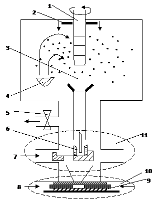 |
1 - a rotating cylinder, cooled by liquid nitrogen, 2 - scraper, 3 - an inert gas (usually not), 4 - Evaporator 5 - valve, 6 - fixing the mold 7 - slide 8 - piston 9 - sleeve, 10 - site of the final compaction at high pressure, 11 - unit prior compaction
Figure 1.1 - Scheme of production of bulk nanomaterials by evaporation, condensation and compaction
During evaporation and condensation of a metal with a high melting point, typically, smaller particle size. Precipitated condensate special scraper removed from the surface of the cylinder and is collected in a reservoir. After pumping inert gas into the vacuum interlocutory (a pressure of about 1 GPa) and final (at pressures up to 10 GPa) compaction nanopowder. This results in a sample with a diameter of 5... 15 mm and a thickness of 0.2... 0.3 mm with a density of 70... 95% of the theoretical density of the material (up to 95% for nanomaterials and to 85% for nanoceramics). Produced by this method compact nanomaterials, depending on the conditions of evaporation and condensation, are composed of crystals (grains) with an average size from a few to tens of nanometers. It should be emphasized that the creation of dense powders are close to 100% of the theoretical density of nanomaterials - the problem is very complex and has not yet been solved, as nanocrystalline powders of bad press, and traditional methods of static compaction fail.
Another method is to compaction of powders produced by the method of mechanical grinding and mechanical alloying. However, there are also problems of compacting nanopowders produced and manufacture of bulk nanostructured samples and blanks with high density.
In applying the method of heat pressing compacting powders of amorphous metallic systems (AMS) is carried out in the temperature range of T near the glass transition temperature T g, which is a significant reduction in viscosity of the amorphous alloy, a few consecutive values. At T> Tr, where Tr (≈ 0,7 Tg) - temperature of the transition from low-temperature heterogeneous plastic flow to the high-homogeneous flow, the material deforms uniformly, and the level required to achieve this stress can be greatly reduced.
However, the development of methods of compacting AMC faces serious problems - the temperature range of the implementation mechanism of the homogeneous flow of low viscosity is rather narrow and is adjacent to the crystallization temperature. Requirements must be satisfied in the process of compacting to prevent crystallization of the AMC. The successful development of methods for the synthesis of massive powder AMC and their products should be able to predict the optimal parameters (time, temperature, pressure) pressing process. The values of these parameters must be determined from the conditions for achieving the desired density compact particular alloy while maintaining the amorphous state. Establishing optimum conditions experienced by compaction - an extremely complex and time consuming task. Therefore, great importance is the theoretical analysis of heat pressing AMC, including clarification of the conditions for obtaining nanoamorfnyh solids.
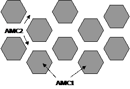
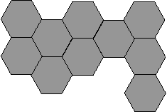
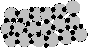
The approach of the particles under external loading occurs visco-plastic flow in the surface layers of inhomogeneous stress fields in the contact interactions of the particles. At the same time there are processes of homogenization of the material of the nanoparticles. Depending on the relative size and structural parameters of the particles and their surface layers (layer thickness and the ratio of the particle radius, and the ratio of viscous-plastic properties of the material layer and the bulk of the particles), the formation of different structural states nanoamorfnyh solids.
If the concentration of excess free volume in the surface layer of the particles is higher than in the bulk, while the surface layer is enriched with impurities embrittle AMC, the viscosity of the material of the layer will be lower than the internal volume of the material and the process of sealing a compact will be due to viscoplastic flow of the material the surface layer. This will form the structure shown in Figure 1.2, a. Surface layer thickness (δ) of the particles should be at the same time sufficient to realize the growth of the contact neck and approach of the particles flow through the material of the surface layer (δ> δr). Parameter δr (r) - the distance particles approach to achieve the required density of the compact set (p) under external pressure (P). In this case, the kinetics of the compact packing material will be determined by the viscosity of the surface layers of the particles.
Otherwise (δ <δr) growth process in the contact neck seal compact will be due to the flow as a material of the surface layer of the particle, and the main material of its volume. In this case, the calculation of the kinetics of densification should use an effective viscosity of the material in contact neck, defined by the rule of mixtures by viscosity material layer and the internal volume of the particle. This will form the structure of the type shown in Figure 1.2b. Subject to the more complex processes such as the formation of regions with different parameters and composition of the topological order on the border of contacting particles (Figure 1.2c).
During compaction compact are also homogenization of particle structure.
For the compact materials with low porosity are used by hot pressing, when pressing occurs simultaneously with sintering. In this case, the pressing pressure is reduced tenfold compared to cold-pressing. Temperature of hot pressing, depending on the nature of the sintered material is in the range 50... 90% of the melting temperature of the main component. However, the increase in temperature leads to a rapid compaction of grain growth and yield of nanostructured state and the consolidation of nanopowders at low temperatures, even at high applied pressures, leading to a residual porosity. Moreover, the problem remains-contamination of samples in the preparation of powders and especially the increase in their geometric dimensions.
 |  | ||||
 |
A Б
В
Figure 1.2 - Structure of solids state nanoamorfnyh
Recommended Reading
1. New materials / VN Antsiferov, FF Bezdudny, LN Belyanchikov and others, ed. YS Karabasova, Ministry of Education of the Russian Federation. - Moscow: MISA, 2002. - 736 p.
2. New substances, materials and products made of them as objects of inventions: Directory / VI Blinnikov etc. - Moscow, Metallurgy, 1991. - 262 p.
3. Rzhevskaya SV Materials science. - M. Bauman, 2000. - 280.
4. Kulikov V.Yu. Textbook for the course "New Materials", KSTU, 2006.
5. Morokhov ID, Cowards DD, Lapovok VI Physical phenomena in ultra environments. - Moscow: Nauka, 1984.
6. Gusev AI Nanocrystalline materials: preparation methods and properties. - Ekaterinburg, 1998.
Control tasks for independent work of the student (theme 5) [1, 2, 3, 7]
1. Advantages and disadvantages of the method of hot pressing.
2. Advantages and disadvantages of the method of warm pressing.
Topic 6: Severe plastic deformation of materials with conventional grain size (4:00)
Plan of the lecture
1. Methods intensivonoy plasichskoy strain.
2. Torsion under high pressure.
3. Equal channel elastic compression.
In this regard, much interest in the production of nanostructured materials by severe plastic deformation, ie large deformations at high applied pressures. The methods SDI is a strong refinement of the microstructure of metals and alloys to nano-scale due to large deformations. In developing these methods, there are several requirements for the production of bulk nanomaterials. First, the importance of formation of ultrafine-grained (UFG) structures with of large-grain boundaries, as in this case, qualitatively change the properties of materials. Second, the formation of nanostructures, uniform throughout the volume of the sample, which is necessary for the stability properties of the materials. Third, the samples do not have to have mechanical damage or destruction, despite intense deformation.
The first work to demonstrate the possibility of bulk nanostructured metals and alloys were made in the late 80's - early 90's RZ Valiev and co-workers, who used two methods to SDI - torsion under high pressure and raznokanalnoe elastic pressing (ECAP).
The design of the torsional deformation under high pressure is based on the principle of Bridgman anvils, where the sample is placed between the strikers and compressed under applied pressure (P) in a few GPa, then attached to the deformation of a very large extent (10 and over). Lower firing pin rotates, and the forces of surface friction force to deform the sample shift. The geometrical shape of the sample is such that the bulk of the material is deformed under hydrostatic pressure, resulting in the samples were not destroyed. The thus-obtained samples are discs of diameter 10... 20 mm and a thickness of 0.2... 0.5 mm. Although their structure is ground deformation after a half-turn, but for the formation of ultrafine uniform strain in the structure is needed several times. The average grain size in the obtained samples, usually of 100... 200. However, the final size of the grains in the structure depends on the conditions of intense deformation - the applied pressure, temperature, strain rate, and the type of the material.
For the production of bulk nanostructured materials using a different method, also based on shear strain - equal-channel angular pressing. In implementing the ECAP billet repeatedly pressed in a special snap in two overlapping channels with the same cross section at room or elevated temperatures, depending on the deformable material. In the most commonly used angles F = 900, each pass corresponds to a high degree of deformation is approximately equal to 1. For the formation of nanostructures is very important is not only the number of passes, but also the direction of passage through channels, depending on which there are several routes of ECAP. An important factor for this method is the preservation of the integrity of samples even maloplastichnyh materials. The implementation of this method can ensure the formation of UFG structure of an average grain size of 200 nm to 500 nm.
In recent years, equal channel angular pressing was the object of numerous investigations in connection with the possible practical applications of bulk nanostructured metals and alloys. Latest developments designed to increase the geometric dimensions of the samples and blanks with a diameter of 60 mm and a length of 200 mm, obtaining long workpieces, the formation of nanostructures in hard-and maloplastichnyh metals and alloys. Much attention is paid to the development of other methods of severe plastic deformation - comprehensive forging, rolling, special, etc., to improve the efficiency of the process.
Recommended Reading
1. New materials / VN Antsiferov, FF Bezdudny, LN Belyanchikov and others, ed. YS Karabasova, Ministry of Education of the Russian Federation. - Moscow: MISA, 2002. - 736 p.
2. New substances, materials and products made of them as objects of inventions: Directory / VI Blinnikov etc. - Moscow, Metallurgy, 1991. - 262 p.
3. Rzhevskaya SV Materials science. - M. Bauman, 2000. - 280.
4. Kulikov V.Yu. Textbook for the course "New Materials", KSTU, 2006.
5. Morokhov ID, Cowards DD, Lapovok VI Physical phenomena in ultra environments. - Moscow: Nauka, 1984.
6. Gusev AI Nanocrystalline materials: preparation methods and properties. - Ekaterinburg, 1998.
Control tasks for independent work of the student (theme 6) [1, 2, 3, 7]
1. Advantages and disadvantages of equal channel angular pressing.
2. Advantages and disadvantages of the torsion under high pressure.
Topic 7 In micro-and nano-electronics (4:00)
Plan of the lecture
1. Overview of semiconductor materials
2. Single-crystal growth
3. Melt extraction method with a continuous replenishment of polycrystalline silicon
Semiconductor materials rightfully occupy a leading position in a number of important materials that determine the level of development of world civilization. They form the basis of elements of modern electronic technology, which today is unthinkable without the scientific and technical progress. With the development of solid-state electronics (and, above all, microelectronics) involves the successful solution of the problems of large-scale computerization and information, the creation of modern communications and television transmission and efficient power conversion, diverse household, medical and special electronic equipment. Important role played by these materials in addressing development of clean energy and refrigeration, a modern monitoring systems of environmental pollution, as well as a highly sensitive sensor technology wide functionality.
Development of solid-state electronics hardware components received much attention in all the advanced countries. Only in 1996, the world production of semiconductor devices in terms of money exceeding $ 160 billion, and in 2000 it amounted to about 300 billion dollars. Each year in the development of this field of science and technology to invest billions of dollars. Achievements in physics, physical chemistry and technology of semiconductor materials and semiconductor materials are essential to progress in the development of solid-state electronics. Our country has traditionally taken (and is now) a leading position in Materials Science and has highly qualified scientists and engineers who are able to date to solve the most complex scientific and technical problems of technology of semiconductor materials.
A characteristic feature of the present stage of development of electronic technology is the scope of its involvement in the direct interests of a wide range of semiconductor materials. The most important are: silicon, gallium arsenide, and a large group of other binary compounds and multicomponent solid solutions, germanium, silicon carbide, binary compounds based on narrow-band and wide-band connections, and touch a variety of thermoelectric materials.
The main material of modern solid-state electronics is silicon. World production of silicon single crystal is 8... 9 tons / year Today, single-crystalline silicon - the most perfect crystalline material from a huge variety of materials ever created by man or nature. Characterized by a high level of quality and a number of other well established semiconductor materials. Modern semiconductor industry - a prime example of the outstanding achievements of the human mind to the development of world civilization, and its further progress related to the solution continuously increasing complexity of scientific and engineering problems.
Next, we consider some of the most pressing problems of the present stage of development of semiconductor technology and materials science.
Single-crystal growth
Single-crystal growth - one of the most critical steps towards the creation of device structures. Carved out of single crystal plates are used either for direct formation based on these integrated circuits and discrete devices, or as substrates in the process of obtaining thin film epitaxial structures. In both cases, the quality of single crystal wafers very high demands.
The main trend in the development of technologies for a wide range of single-crystal semiconductor is grown larger diameter ingots, while the continuous strengthening of requirements for perfection of the crystal structure and the uniformity of distribution of electrical characteristics defined in the bulk material. In the case of silicon, it is about getting dislocation-free single crystals with a diameter up to 450 mm in the case of GaAs, InP, GaSb, InSb, CdTe, etc. - malodislokatsionnyh single crystals with a diameter of up to 100... 150 mm.
The most universal method of growing single crystals of large diameter is the Czochralski method. Increasing the diameter of grown single crystals and the need to ensure high economic efficiency of the process chain in the crystal - a plate requires a precision of heavy, high-performance and fully automated plant growth. If, for example, in the production of silicon single crystals with a diameter of 200 mm are used to load the oven to 150 kg and a diameter of 300 mm - 250... 300 kg, moving to build single-crystal 450 mm requires a growth equipment to load 550... 600 kg. The diameter of the quartz crucibles used increases to 0.9... 1.0 m.
At present, the main products in the world market are single crystals of semiconductor silicon wafers and 150 and 200 mm. In 2001, the leading silicon manufacturers began to produce dislocation-free single crystals and wafers 300 mm in diameter compared with those for 200 mm wafers, and further significantly exceed them. Also, keep in mind that is already developed and pilot-testing of industrial technology for growing dislocation-free single crystals (and manufacture of these plates) with a diameter of 400... 450 mm.
Tackling the growing single crystals of large diameter by successive increase in the mass of initial load and size of the quartz crucibles at each new stage of increasing the diameter of the ingot becomes less cost-effective due to the significant increase in energy consumption, cost, crucibles and increased costs to provide safe working conditions. From this point of view, special attention should melt extraction method with a continuous replenishment of granular or particulate polycrystalline silicon. The main advantage of this method is the ability to grow crystals of the large mass of relatively small and constant over the volume of the molten bath in the crucible of smaller size. There are other fundamental advantages: to provide uniform distribution of impurities increase the length and cross s
| <== предыдущая | | | следующая ==> |
| Культура Росси во второй половине 19 века | | | Билет 31 |
Date: 2015-07-23; view: 369; Нарушение авторских прав; Помощь в написании работы --> СЮДА... |